

There are many types of circuits for button switches, and today there are two types of time-delay lamps for buttons, 4011 chips for the former and 4017 chips for the latter. By understanding the two chips, the principles of these circuits can be quickly understood. Where these two chips are not known, reference can be made to a simple description of the cmos digital integrated circuits, in which their use is described in detail。
Key control timer -- 4011 chips
The auto-heat multi-organizer is an unstable circuit, but there are two unsustainable staggers that can be continuously transformed into oscillations, as described in the previous article. The following is a single, stable circuit with a non-door composition of the rc differential. The so-called single-state circuit, i. E. A state of stability and a temporary state of stability that, under the control of the input signal, can be transformed from a state of stability to a state of temporary stability and, after a certain period of time, automatically return to a state of stability, the duration of which is determined by the parameters of the element. A chart of the principles of the circuit follows。
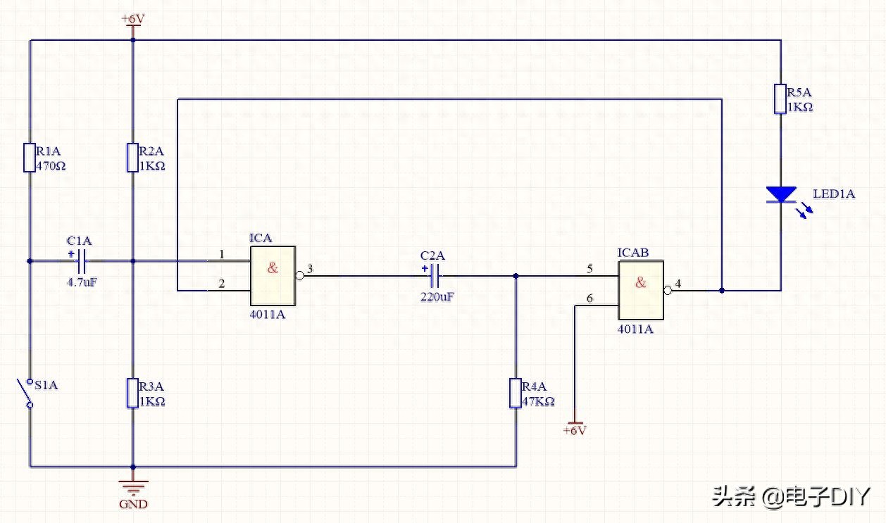
Key control timer simplification diagram
Two are equivalent circuits, one of which is 4011 chips, and the next is a complete 4011 chip circuit。
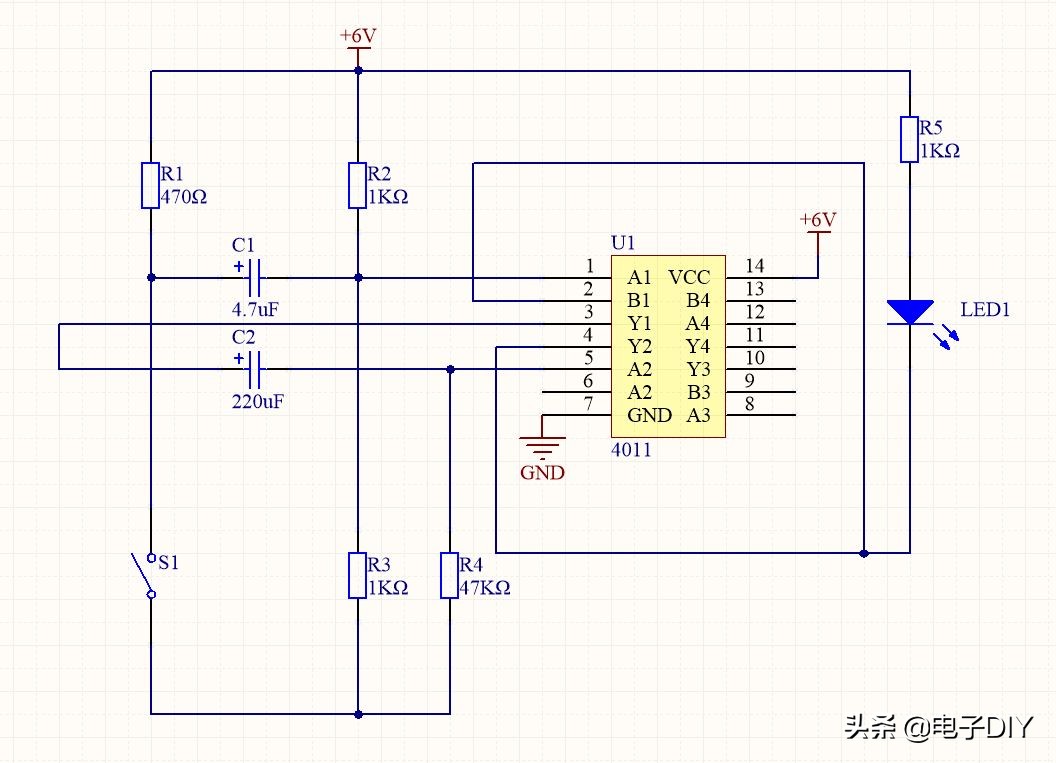
Keys control the time-delaying lights
Brief description of the rationale
The circuit consists of a single steady circuit with a non-gate ic1a, ic1b and c2 and r4, a negative pulsed circuit with a button switch s1 and c1 and a led1 and r5 displaying the circuit. When the power is just connected and s1 is not closed, the power is charged to the capacitor c1 through the electrical resistance of r1 and r3, the left side of c1 is positive, and the r2 and r3 form a subvoltage circuit, which gives the ic1a input end foot 1/2 of the power voltage, i. E. Around 3v, higher than the conversion voltage of ic1a. At this point, the sixth foot of ic1b is attached to the positive end of the power supply, the sixth foot is high, the fifth foot is low because of the blockage of r4 by electrical means, so the fourth foot of ic1b at this time is high, which is loaded to the second foot of ic1a at the same time, so that the third foot of the output of non-ic1a is low。
When the button switch s1 closes, the charge already filled on the c1 is blocked by r3 discharge, the discharge direction on the r3 is from the bottom up, contrary to the current direction originally used as a sub-voltage circuit, thus receiving a negative to the top pulse signal at the first foot of the ic1a, at which point the third foot of the ic1a output will turn to a high electrical level, the fifth foot of which is sent through c2 to ic1b, and the 5th foot of the ic1b will be high, as the two ends of the electron voltage cannot be mutilated, so the fourth foot will be flatened to a low level, driving led1 point, and the electrical path will be stable from a steady state to a temporary state。
As c2 recharging continues, the 5th foot of ic1b will gradually be reduced to the flip level of ic1b, and the 4th foot will return to high level, led1 will be extinguished and the circuit will be stabilized。
The output pulse width of this micro-specified single-state circuit is fixed, i. E. The time of continuous output of high-level level after the ic1a trigger is fixed, while the duration of led1 brightness will be determined by the timed components c2 and r4 and its delay formula is t=0. 94 x c2 x r4; generally, r4 has a relatively small range of values and c2 can be larger。
Experimental tip
S1 in the circuit is a lockless button switch, which is tested by placing the switch in " on " , closed and then disconnected to simulate the process of the switch. We can see from the experiment that the length of s1's closure, even holding it down, has no effect on the width of the output pulse, and the brightness of led1 does not change。
The 1st-foot shape of ic1a can be observed with an oscillator, if available, and there will always be more or less, or a cut-off, in the s1 closed moment, a phenomenon that is prevalent in the closed moment at a mechanical switch point, generally referred to as “diverse”. However, after a single-stabilized state has been lighted, it is possible to output a steep, negative pulse signal with a certain width, which is the function of the micro-specified single-stabilized circuit signal wave width and shape。
There are four sets of second input ends and non-doors in the 4011 chip, only two of which are used, and the remaining two sets of unused non-doors, whose input ends are not suitable for suspension, should be attached to high or low electrical levels in order to prevent the uncertainty of the input level due to the suspension, leading to a logical error in the chip and affecting the stability of the circuit。
Key control switch -- 4017 chips
This is a key control switch that consists of a decimal count 4017. A chart of the principles of the circuit is shown in the figure。
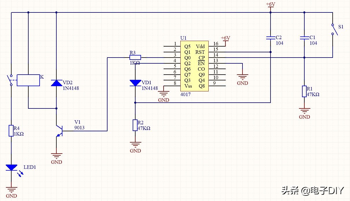
Key control switch rationale
Brief description of the rationale
Following the power connection, c1 was recharged by r1 and filled with electricity in a short period of time. The r2 and c2 form an on-the-post circuit, and c2 can be seen as a short circuit when electricity is available, so the 15th foot rst at the end of u1 is at high level, u1 is restored, c2 is charged in a relatively short period of time, the 15th foot of u1 is restored to low level, at which point q0 output high level, passing through the base pole of r3 plus v1, the v1 conductor, the relay k-sorption, the led1 point indicating that the alleged circuit is connected. The q1-q9 output end of u1 is low level。
When pressing switch s1, c1 is rapidly discharged, the 14th foot of u1 gets pulsed up, triggers u1 start count, and the output of q0 is converted from high to low level. Q1 output high level, and q2 maintains low level, at which point v1 is closed, relay k is released and led1 is extinguished, indicating that the power supply is allegedly stopped. Once the switch s1 was released, c1 was again charged with electricity。
When you press s1 again, c1 will release again, the 14th foot of u1 will receive a count pulse again, triggering the u1 count again, and q0 and q1 output will be low level, q2 will output high level, which will revert to u1 after vd1 plus u1, 15 foot rst at the rear, so that the output of q0 will become high level, q1 and q2 output low level, v1 will again conduct, relay k-suction, led1 point indicating that the alleged circuit will again be powered. Thus, every time the output of s1, q0 was pressed, the alleged circuit was turned over or shut down。
Experimental tip
During the course of the circuit work, when presses s1, c1 discharges, when the s1 is released, and after a short period of time, c1 refills the electricity, so that the 14th foot of u1 will be low, during which time any mechanical shaking on the switch s1 will not produce a second technical pulse, thus providing protection against shaking. Other output ends of 4017 are unused and can be suspended。
Little partners who have not yet understood it, take more time to look at it, the circuits are easy, there are not many devices, the production is easy, and understanding is slow。